I finally managed to work on the Imgotag project!
Suggested music:
PostmodernJukebox - Seven Nation Army (ft. Haley Reinhart)
Robin Schulz - Sugar (ft. Francesco Yates)
Part 2
The Complete Circuit
If you want to feel the same thrill I had, here you have the datasheet files and the aligned Photoshop image:
The board is really similar to this datasheet diagram, but peeking through the PCB layers I discovered that there are some differences in pins 5 to 8, connected to other capacitors or power rails, probably they had their custom EPD made.

Still, there is a thing that I can't figure out: It is obvious that this board has A LOT of unused space, and this is a plus, as it adds flexibility to accommodate late changes or different variants, but why did they do this:
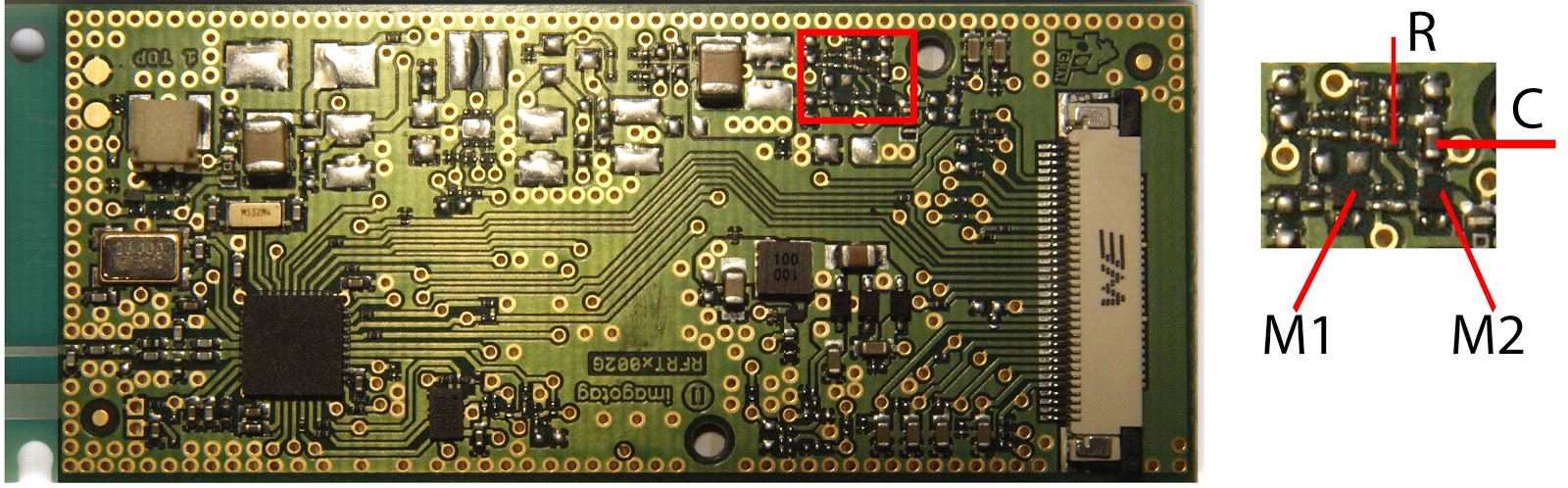

We have two pMOS in series, the second one retarded with an RC lowpass.
Simply put: it takes a little more time to switch the second transistor on.
I understand the need for an RC to limit the inrush current: coin cell batteries are known for having high series resistance; not having a "soft start" protection might bring the Vdd too low and trigger the brown-out of the MCU!
But why TWO pMOS? If it wasn't an obliged choice or a mistake, I have no idea.

