I finally managed to work on the Imgotag project!
Suggested music:
PostmodernJukebox - Seven Nation Army (ft. Haley Reinhart)
Robin Schulz - Sugar (ft. Francesco Yates)
Part 2
The Complete Circuit
If you want to feel the same thrill I had, here you have the datasheet files and the aligned Photoshop image:
The board is really similar to this datasheet diagram, but peeking through the PCB layers I discovered that there are some differences in pins 5 to 8, connected to other capacitors or power rails, probably they had their custom EPD made.

Still, there is a thing that I can't figure out: It is obvious that this board has A LOT of unused space, and this is a plus, as it adds flexibility to accommodate late changes or different variants, but why did they do this:
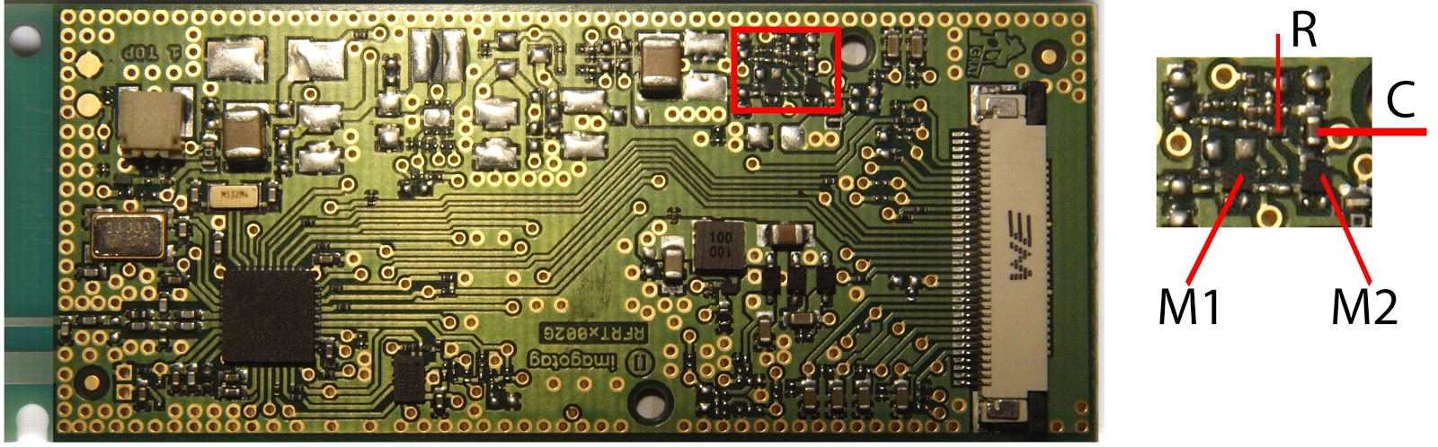

We have two pMOS in series, the second one retarded with an RC lowpass.
Simply put: it takes a little more time to switch the second transistor on.
I understand the need for an RC to limit the inrush current: coin cell batteries are known for having high series resistance; not having a "soft start" protection might bring the Vdd too low and trigger the brown-out of the MCU!
But why TWO pMOS? If it wasn't an obliged choice or a mistake, I have no idea.


At this point, the only thing needed is to attach an SPI master to our display and see what we can send to it.. Or so I thought!
The datasheet is not very clear in explaining how the communication happens: the signals are named SCL and SDA (as in I²C) but they clearly state "SPI" all over the document...
As inputs we need to provide MOSI, CLK, CS, D/C, Power switch and reset to the display.
The display sends back a BUSY signal telling us when the EPD is ready.
At this time I had to decide weather to use a 3.3V device to communicate with our EPD or to use a level shifter.
I have several ARM cortex M that can serve the purpose, unfortunately setting them up is really a PITA (I love using them, and they are for sure a great tool and a real challenge), but I have no time to loose now, and I had an Arduino accumulating dust in a drawer..
Given that the logic level high of the Arduino is around 2V, I can connect the BUSY line directly to the digital input.
For our testing purposes the power can be always on (Vg of the pMOS pulled at ground) and since the chip select is a slow signal, we can use a simple 2.2KΩ-3.3KΩ voltage divider without worrying too much about signal integrity.
From some previous projects, I had a 4 channel level shifter, which I quickly set up with a jungle of jump wires:

After connecting everything from the backside test pads, we can send some SPI signals and see.. Distorted waveforms on our scope, inconsistent data on the logic analyzer!
I was groping in the dark trying to figure out if my long, thin cables could have distorted the square waves that much.. Maybe ground impedance issues? Maybe ringing? Maybe the logic shifter is malfunctioning?
I check the frequency of the square wave, and even the 5th harmonic is way below 10MHz, so no issues with that.
I swap the level shifter with a bunch of voltage divider resistors, nothing.
This is the perfect time to go to the kitchen and grab a cup of tea, sit back and think...
I check and recheck the connections, and only after a couple measurements with the multimeter I notice the zero impedance path between CLK and MOSI. Douch.
I had misfollowed traces on the PCB and soldered the adjacent test pad..
So now that we have everything attached and tested, it is time to try and send some signals to the EPD!
See you soon with part three!
Epongenoir
Did you manage to get something going with this? I also have something that seems a newer version of the same thing. I managed to program the CC2510 with some custom code that drives the EPD. Next step: get wireless packets in and out.
ReplyDelete